
Optical mask lithography is a technique based on the behavior of some substances, like thin photoresist layers, under illumination with ultraviolet light. The integration density and properties of microelectronic devices depends on their linear dimensions. During the lithographic fabrications process they are defined by the opaque or transparent patterns of the microstructures that are imposed on the photomask and used for the photolithographic exposure. The UV light illuminating the lithographic masks projects the patterns on the sample with light sensitive layer. The resolution of the mask-based lithography methods is mostly determined by the quality of the mask. Laser writing technique is an attractive alternative for the photomask fabrication [1].
In this work a UV mask was produced employing a femtosecond laser micromachining utilizing FemtoLAB workstation and third harmonic of Yb:KGW femtosecond laser Pharos. Ablation resolution tests in metal oxide films on glass substrates were organized with SCA v2.6 software. Owing for optimal microstructure resolution the pulse density, pulse energy, attainable translation speeds and other related laser processing parameters were varied. Resulting structures and their quality were analyzed under optical microscope. Typical geometrical shapes, namely lines and circles of μm range dimensions ablated in metal oxide film are depicted in Fig. 1.
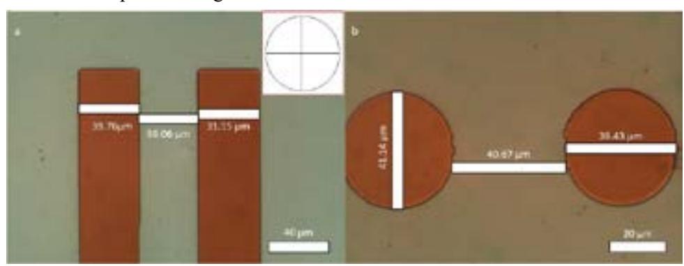
Optimization of the ablation procedure was carried out employing a test pattern consisting of straight and curved intersecting lines indicated in the inset of Fig. 1 a. Preliminary ablation experiments enabled us to produce a lithography masks depicted in Fig 1 a and b with a mark speed of 0.5 mm/s a jump speed of 10 mm/s and a pulse density of 6000 pulses/mm. The optimization of the patterning speed is still in progress.
This research was funded by the European Social Fund under the No. 09.3.3-LMT-K-712 “Development of Competences of Scientists, other Researchers and Students through Practical Research Activities" measure, grant No. 09.3.3.-LMT-K-712-10-0214.