
Graphene is a promising material with high charge mobility [1-3]. The substrate material has a significant negative influence on the charge carriers mobility. Silicon carbide well established as substrate in graphene technology. However, the mobility of charge carriers in such systems is worse than the theoretical calculations of a pure graphene sheet [2, 3]. The space charge inhomogeneity (so-called charge puddle) leads to degradation of the graphene electronic properties [4]. Physical characteristics leading to the occurrence of electron-hole puddles not identified uniquely [1, 5].
Silicon carbide (SiC) has unique electrical properties, due to which SiC is used in micro- and nanoelectronics. Silicon carbide has in the manufacture of high-power rectifier diodes, microwave diodes, thermistors, field-effect transistors with good frequency properties, as well as high-energy particle counters that are capable of operating in chemically aggressive environments.
Calculations were performed by quantum-mechanical simulation without taking into account of Van der Waals forces which are significant in layered structures. Calculations were performed based on the density functional theory (DFT) [6]. All of calculations have been carried out using VASP (Vienna Ab initio Simulation Package). The projector-augmented wave (PAW) potentials [7] and Perdew-Burke-Ernzerhof (PBE) functional [8] have been used. A cutoff energy of 520 eV. The atomic structures were relaxed until the forces on all unconstrained atoms were smaller than 0.01 eV/Å. A vacuum layer of 17.5 Å along z direction was constructed to eliminate the interaction with spurious replica images. The calculations were carried out without spin polarization. Integration in reverse energy space was carried on the $7 \times 7 \times 7$ k-points grid determined by a fine grid of gamma-centered method. Static self-consistent calculations were performed using the tetrahedron method and Bloch corrections. The DFT-D3 method of Grimme [9] demonstrated the smallest difference between the calculated and experimental magnitude of lattice constants and have been used for further calculation. Fig. 1 shows charge distribution in graphene on silicon carbide substrate.
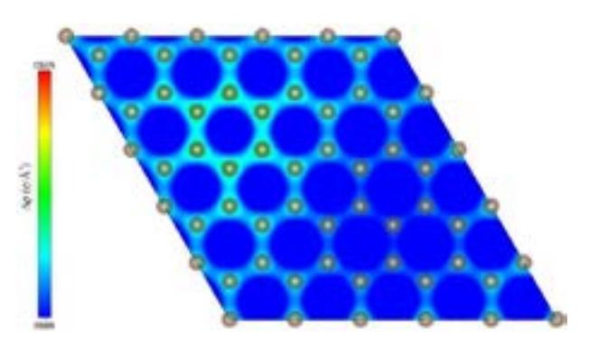
Interlayer distances and adsorption energy were calculated. The absorption of graphene on the surface of silicon carbide with silicon dangling bonds is most energetically favorable ($E_{ads} = -7.2 \text{ kJ/mol}$). The distances between the graphene layer and the surface of the substrate range from 3.23 to 3.35 Å, which corresponds to physical adsorption with a strong influence of the Van der Waals forces.
The band structures were calculated for the graphene on silicon carbide surface. Changes in the states of graphene under the action of a substrate are observed in the immediate vicinity of the Fermi level. The Fermi level is shifted toward to the valence band, which indicates a small redistribution of charge on the substrate. Overflow of charge occurs on the near-surface silicon atoms. Energy gap arises width 86 meV between the bonding and antibonding $\pi$-zones of graphene. Electronic structure of adsorbed graphene has no changes.