The increasing need for efficient light sources emitting at different wavelengths forces engineering of novel compounds and progress in material science. One of the main problems of modern semiconductor lasers – bandgap sensitivity to the temperature deviations, makes such laser systems require additional cooling, reducing their efficiency, compactness and affordability. It was shows previously, that incorporation of 1% of Bi to the GaAs lattice reduces bandgap by up to 88 meV [1]. Moreover, spin-orbit splitting increases at higher Bi fractions, which opens up a possibility to suppress Auger and other non radiative losses [2]. Finally, dilute bismide alloys were shown to have unusually low bandgap temperature dependence compared to widely used III-V compounds [3]. These three properties make GaAsBi and other bismides attractive for various optoelectronics device applications, including lasers [4].
This study focuses on research of GaAsBi alloy as an active region of NIR lasers, emitting at around (1-1.2) μm. The aim of this work is to optimize technological growth conditions of GaAsBi Multiple Quantum Well (MQW) structures in order to achieve high intensity Photoluminescence (PL) signal. The influence of different element ratios, growth rate and temperature, QW and barrier layer thickness, Be dopant concentration to the optical and structural properties was investigated.
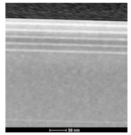
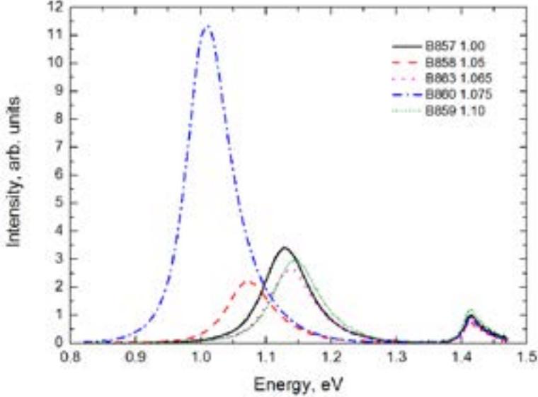
GaAsBi MQW structures were grown by molecular beam epitaxy (MBE) on semi-insulating GaAS (100) substrates. High resolution X-Ray Diffraction (HR-XRD) and Transmission Electron Microscopy (TEM) were employed to evaluate crystalline structure and content of bismuth (Fig 1). Atomic Force Microscopy (AFM) was used to determine surface quality, while PL measurements were performed to investigate optical properties (Fig 2).