THz imaging is a promising technology for applications in security, medicine or pharmacy [1]. Improvement of optical elements for THz frequency radiation is important for minimizing the size and cost of imaging systems. One way to make THz optical systems more compact is to use diffractive optical elements – Multilevel Phase Fresnel Lenses (MPFLs). One way to produce MPFL elements is direct laser ablation [2]. Laser processing allows producing the desired elements in a relatively simple one-step fabrication without the use of auxiliary masks or materials.
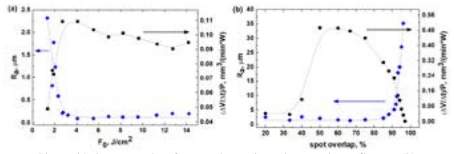
In order to make MPFL production cost-effective it is important to have a sufficiently short fabrication time. Material removal rate in direct laser ablation process depends on the irradiation parameters such as laser fluence at the center of the focused laser spot ($F_0$) and laser spot overlap. At the same time fabrication quality such as roughness of the ablated surface ($R_a$) also depend on these parameters [3].
In this work, influence of various laser processing parameters on the transmission of THz radiation was investigated. Using 1064 nm wavelength picosecond and nanosecond laser pulses and 100 kHz pulse repetition rate, 6 x 6 mm2 craters on a monocrystalline silicon (100) wafer were ablated varying laser fluence and spot overlap. Thus, silicon samples with different surface roughness and ablation efficiencies were prepared (Fig. 1).
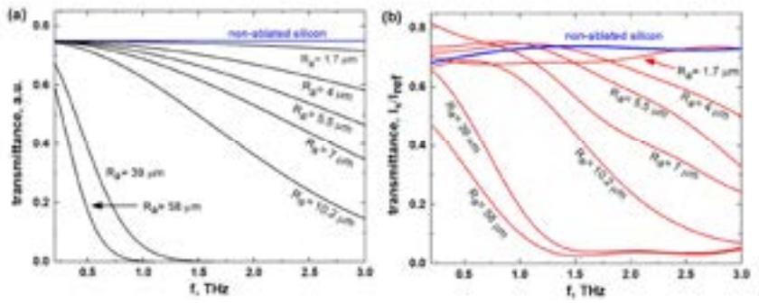
Transmittance (T) of the ablated silicon plates in THz radiation frequencies were compared with theoretical model which predicts transmittance losses due to surface scattering:
$$T = (1 - R_0) \exp\left[-\left(\frac{4\pi R_a}{\lambda}\right)^2\right],\tag{1}$$here $R_0$ is reflectance of non-ablated silicon, $\lambda$ – wavelength of scattered light. Theoretical predictions and measured transmittances using time-domain spectrometer for samples with various surface roughness are shown in Fig. 2.