
InGaAs-based bow-tie diodes for terahertz (THz) range are found to be well-suited for development of compact THz imaging systems [1]. To further optimize design for sensitive and broadband THz detection, one of the major challenges remains to understand influence of growth conditions and role of defects for device operation. We present detailed study of photoreflectance and THz sensitivity of InGaAs bow-tie diodes. The diodes are fabricated from InGaAs wafers grown by molecular beam epitaxy (MBE) on semi-insulating InP substrate under different technological conditions. Photoreflectance spectra indicated presence of strong built-in electric fields reaching up to 49 kV/cm. Furthermore, varying bias current, we evaluated fabricated devices for optimal room temperature operation in THz range with respect to signal-to-noise ratio.
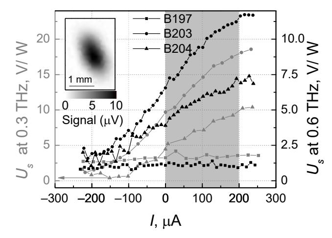
Figure 1 depicts the sensitivity as a function of current for all types of the studied samples at frequencies of 0.3 THz and 0.6 THz. As it is seen, sensitivity of InGaAs bow-tie diodes fabricated from the wafers B203 and B204 increases while raising the current and reaches 17.5 V/W and 10 V/W at 0.3 THz and 12.5 V/W and 7 V/W at 0.6 THz, respectively, at the bias current of 0.2 mA. Higher voltage sensitivity of the detector B203 is caused by the larger asymmetry in the IV curves and stronger built-in electric fields in comparison to other studied samples. Raster scan of THz beam profile at 0.6 THz (inset in Figure 1) illustrates the suitability of the diode for THz imaging aims.
To conclude, the THz detectors layers grown with beam equivalent pressure In/Ga ratio equal to 2.06 are found to be well suited for fabrication of room temperature bow-tie THz detectors enabling sensitivity of 13 V/W and noise equivalent power (NEP) of 200 pW/$\sqrt{\text{Hz}}$ at 0.6 THz due to strong built-in electric field effects [2].