Block copolymers (BCPs) usually consist of a few blocks, that are covalently bonded. They are a class of self-assembling materials, that drew much attention thanks to its unusual properties. Worth mentioning is the self-assembly phenomenon. It is a powerful motif, in which BCP tries to minimize energy and thus forms diverse structures such as lamellaes, cylinders or spheres. Also, parameters of obtained nanostructures can be easily tailored by changing composition and molecular weight of BCP, which affects the periodicity of BCP thin films. When one combines it with large scalability, it makes BCPs great candidates to become widespread in the semiconductor industry as organic matrices for fabricating metal-semiconductor nanostructures.
In order to achieve that, the use of a method to control its ordering parameters, that comes together with the reasonable time of a process is essential. An easy and cheap technique is thermal annealing, but the long time of a process limits its wider application in industry. Another option, that shows better quality along with the shorter process time is Laser Zone Annealing (LZA) method. In this technique very high temperature gradients are induced, while the focused laser beam locally heats the substrate with the polymer ontop [1]. As a result, uniaxially aligned BCP films are obtained.
There are many ways to deposit metal or semiconductor compounds. To obtain metal nanostructures Aqueous Metal Reduction (AMR) method is utilized. A BCP film is immersed in a solution of complex metal salt (e.g. K2PtCl4 for Pt) dissolved in an acidic environment. Via electrostatic interaction anion bounds with a favourable functional group in BCPs [2]. Oxide semiconductors might be deposited by the Sequential Infiltration Synthesis (SIS) technique. Sequential Infiltration Synthesis (SIS) is a variation of an Atomic Layer Deposition (ALD) method, where two gaseous precursors are introduced to the reaction chamber separately and homogenously saturate the surface. During exposure time each precursor infiltrates the bulk of polymer material and reacts with functional groups (e.g. carbonyls). Consequently, the inorganic nanomaterial precursor is embedded in a polymer matrix [3].
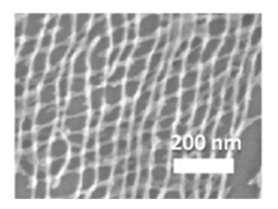
Combining these methods allows one to fabricate multilayered metal-semiconductor nanomeshes. In our work, we were able to successfully obtain double-layered heterostructures, that were examined by Scanning Electron Microscopy (SEM) and Atomic Force Microscopy (AFM) measurements. These investigations may pave the way in the development of more efficient miniaturized chemical sensor with higher sensitivity and lower power consumption, comparing to the currently sold devices.