
Graphene is the best-known 2D material because of its extraordinary structural, physical, and chemical properties, and the industrial interest in investigating graphene applications in many different areas, such as electrooptics, photonics, plasmonics, optoelectronics [1], grew rapidly over the last decade. Simultaneously, different routes of production and synthesis of graphene are available with varying level of successfulness. Nevertheless, the development of graphene applications is fairly slow process, and possibly the main cause for this is not optimal, rather poor quality of the graphene produced by many companies in the world, which is an indisputable fact [2]. Therefore, it is very important to evolve and improve tools and methods for graphene quality exploration with regard to present defects and disorder.
At a moment, one of the best developed methods to characterize graphene films is Raman scattering spectroscopy for being nondestructive, fast, of high resolution, and so far providing the maximum structural and electronic information about graphene layers [3]. One the other hand, ultrafast spectroscopy method widely used in other fields, until now was not sufficiently explored for thorough systematic defects and disorder analysis of graphene. In our research we present ultrafast transient absorption spectroscopy (TAS) technique as an efficient tool to evaluate the quality of graphene layers. Understanding the influence of such defects on the charge carrier dynamics and excited state relaxation pathways is a key to modifying the optoelectronic properties of graphene-based devices.
Employing a widespread microwave plasma enhanced chemical vapor deposition (PECVD) technique, large area graphene layers were synthesized in two ways – directly on insulating substrates (fused silica) initiating the formation of vertical graphene nanosheets (VNGs), and on metallic catalyst (Cu foil) for production of continuous films possessing an intrinsic planar structure. These structural differences were identified by Raman scattering spectroscopy measurements, additionally revealing different prevailing types of defects within the analyzed graphene films, which are edges and boundaries for VGNs and vacancy-like defects for transferred planar graphene layers (Fig. 1). The detailed analysis and comparison of structural, electrical, optical, morphological, compositional and electro-optical properties of graphene layers depending on preparation method was carried out by utilizing transmission line method, UV-VIS spectroscopy, AFM, SEM, XPS.
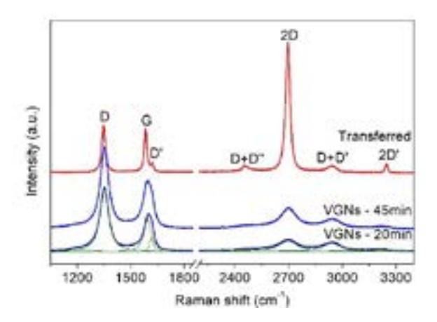
We used TAS technique to analyze excited state relaxation dynamics (typical relaxation times, absorbance spectral dependences) in graphene, and how the excitation phonon energy influences these dynamics. The analysis has shown that TAS relaxation kinetics for the measured samples is fastest under excitation with wavelength of 700 nm. We basically measured hot electron cooling dynamics, that originates from electron-optical phonon interaction, leading to phonon-phonon interaction. These relaxation durations have given the information about the defects as well. The better understanding of how defects influence excited state dynamics in graphene might lead to the creation of methodology based on TAS for defects investigation compatible with Raman scattering spectroscopy.