Nowadays great attention is given to ecological problems such as global warming. Population growth increases energy demand and most of this energy comes from fossil fuels. This energy source causes carbon dioxide emission, which leads to climate change [1]. Due to this, it is very important to search alternative energy sources or develop such power station, which use wind power plants or solar cells [2].
Semiconducting materials are used for solar cells and it is very important to synthesize compounds with good electrical properties and high efficiency. These days a good characteristics shows ternary semiconductor layers such as Cu2SnS3, Cu3SnS4, CuInSe2 or CuGaSe2. CuInSe2 layers have a great absorption coefficient but indium is rather expensive in case of this it is more economical to use copper [3, 4]. There is many deposition techniques, which let to deposit such binary or ternary layers (thermal crystallization of evaporated, chemical bath deposition, atomic layer deposition). Furthermore, composed layers can be modified by other element incorporation, for example copper could be chemically incorporate into thin films of indium selenide. This process allow to change properties of primary film [5].
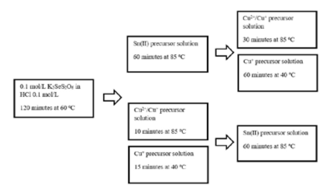
In this work tin selenide layers with incorporated copper were formed on hydrophilic polymer polyamide 6 surface by simple and economic sorption-diffusion method. For the selenization polymer was immersed in 0.1 mol/L selenotrithyonate ($K_2SeS_2O_6$) in HCl 0.1 mol/L solution for 120 minutes at 60 °C temperature. In the second stages, samples were treated with tin (II), copper (II/I) and copper (I) precursor solutions at different conditions (Fig. 1). Structural and elemental composition of the obtained layers were investigated by X-ray diffraction (XRD) analysis.