
The variation of electrical, surface charge and strain properties of CVD graphene based Au and Ni contacts were investigated after samples were exposed to air. Long thermal treatment of samples was performed to compensate the atmospheric influence in graphene structures, moreover thermal process induced changes were investigated analyzing the changes of strain and doping in graphene sheet. Raman spectroscopy and Kelvin force probe microscopy were exploit to observe charge doping, strain and work function in graphene on SiO2 substrate and metal films. Values of these characteristics before and after sample thermal treatment were compared.
The properties of the planar junction between graphene layer and thin film metal structures are important for formation of the electronic devices integrating the structures of the two-dimensional materials. However, the properties of the graphene-metal contacts are still weakly controlled in the large area device fabrication. We demonstrated an approach acceptable to characterise the long distance distortion area produced by the metal contact edges in the graphene monolayer. The systematic analysis of the Raman maps of the graphene is performed aiming to describe the changes in the graphene monolayer produced by the technology dependent parameters in the planar structures used for the measurements by the circular transmission line method. It was proved that Au contacts produce the compressive strain in the graphene layer in the distances up to about 2-4 μm from the contact edges. The transition between the n and p-type of the doping is combined with the compression strain in the long distance graphene distortion area close to the Ni-contact edges. An equivalent electrical circuit is proposed for description of the graphene distortion area near the contact edges.
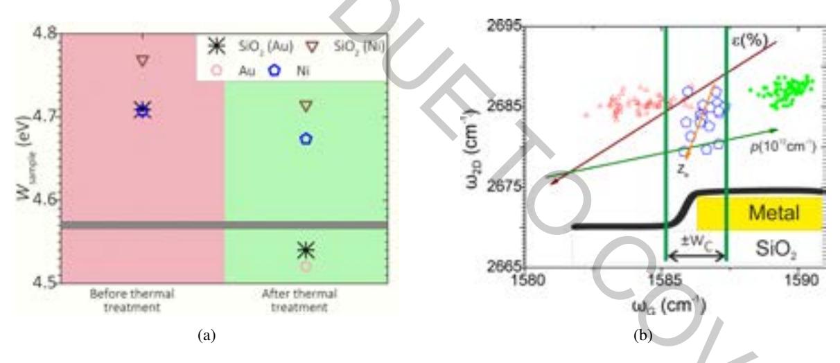
The largest decrease of $W_{Gr}$ of CVD graphene observed in Au contacts. Raman analysis indicated the increase of p-type doping in graphene on metal films (on both Au and Ni). Graphene on SiO2 substrate demonstrated higher values of p-type doping. The correlation between doping in graphene layer and variation of resistance implicated the idea that atmospheric induced changes occur mainly in graphene layer on SiO2 substrate. Graphene doping and strain changes caused by exposing to air on metal films were minor.
Based on the principles of the method it was demonstrated that the metal contact edges produce the changes in the properties of the graphene monolayer at sufficiently large distances from the edges. The distortion of the graphene can be identified at the distances from 2 μm to more than 8 μm. The compressive strain was detected for all the samples in the close vicinity of the contact edges.