Over the last decade, halide perovskites have emerged as promising materials to supersede conventional AIIIBV semiconducting nano- and microstructures for photonics applications. Great interest in perovskites is caused by their unique structural and photophysical properties such as defect tolerance, highly efficient absorption and emission, and long diffusion length. Moreover, these materials tend to form regular shaped nano- and microcrystals - optical resonant cavities. The electromagnetic field in such cavities is distributed in the form of resonant modes (e.g. Mie, Fabry-Pérot, or whispering gallery modes) and mediates laser action because of both optical gain and refractive index of the medium are sufficient. Generally, perovskite resonators exhibit high-quality lasing ($Q_{las} \sim 10^3 - 10^4$) at low threshold power. [1, 2, 3, 4, 5] The outcoupled light propagates in certain directions defined by the shape of the resonator. However, the improvement of laser performance as well as light management could be realized by integrating the perovskite cavities with various nanomaterials.
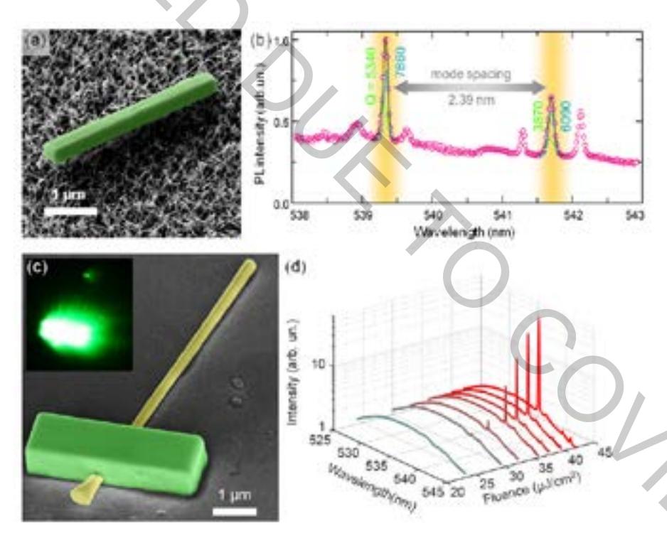
Herein we report on CsPbBr3 nanowires deposited on nanostructured indium-tin-oxide substrates (Fig. 1a) by using a simple wet chemical approach. Surface passivation of the substrates is found out to govern the regularity of the perovskite resonators shape. The nanowires show room-temperature lasing with quality factors that are 3-4 times higher than that of similar structures on a flat indium-tin-oxide layer (Fig. 1b). Concerning the light management, we show simple integration of CsPbBr3 microlasers with GaP nanowaveguides (Fig. 1c) resulting in the direct output of coherent light from the end facet of the latter (Fig. 1d). Importantly, long-range guiding of visible light could be realized in CsPbBr3-GaP structures since GaP exhibits low ohmic losses in the range of perovskite photoluminescence.