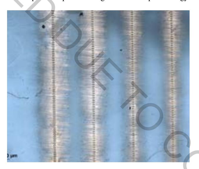
Microelectronics has been rapidly evolving as the most in-demand field of electronics because of the ever-increasing demand for inexpensive and lightweight equipment. Materials such as silicon and copper are commonly used in manufacturing microelectronics. Therefore, direct metalization of bare glass with copper is required to reach the full potential of low-cost benefit [1]. Two step process is needed to obtain precise microstructures in glass before metal deposition: 1) create structures in glass using femtosecond laser 2) use alkali etching for via holes in the material. In this report we research a fundamental material challenge, associated with copper-to-glass adhesion.
Raman spectroscopy is a powerful method for determination of glassy material analysis. The chemical composition and structure of molecules influence the scattering and no two of the spectra being exactly similar [2]. Using Raman spectroscopy in D263 glass we indicate different chain lengths of SiO4 tetrahedral structures. These links are specified in Qn parameter, which describe quantity of bridging oxygens in the structure. Using laser pulses these tetrahedral chains can be contracted by creating shorter structures than the origin. Therefore, laser densified area acquires a greater reactivity to Potassium hydroxide (KOH) etchant and facile Si-O-Si cleavage [3], consequently we are observing a selective chemical etching. These two processes take place in designing desired microstructure in dielectric material.
Finally, creating laser and chemical etchant modifications in glass a selective metal deposition was witnessed. It has been a clear connection between metal deposition speed on the glass and laser pulse energy as well as chemical etching.