In recent years, graphene has become one the most studied nanomaterials due to its intrinsic optical, mechanical, thermal and electronic properties. This proposes many possibilities for creation of novel graphene based optoelectronic devices [1] which encompass all the previously mentioned qualities. To achieve correct geometry, thickness and most importantly large surface area of graphene sheets, microwave plasma enhanced chemical vapor deposition (MW-PECVD) is known as a feasible method for direct growth of graphene on desired substrates. However, despite decreased production times and the ability to ensure correct growth dynamics, MW-PECVD has a huge negative impact on graphitic structures – defect density tends to be noticeably higher compared to graphene synthesized using other techniques [2].
To tackle this issue thermal annealing is rather straight forward method, which usually increases the overall quality of graphene by reducing the number of defects and other structural deformations, however there are other predominant effects, such as doping and strain effects, which could damage the sample [3]. To investigate these structural changes, Raman spectroscopy is a useful technique to determine changes in graphene quality. By comparing $I_{2D}/I_G$ we can establish if the deformations are compressive of tensile and $I_D/I_G$ is used for direct defective site related behavior.
In this work, four graphene samples were grown on Si(100) substrate, using MW-PECVD system (IPLAS Innovative Plasma Systems GmbH). Thermal annealing of samples was accomplished accordingly: in 200-800°C Ar environment, in 300-400°C $N_2$ environment and using 300°C in vacuum. All annealing's were performed for 30 min. The characterization of graphene samples was carried out using Raman spectrometer (Renishaw inVia, 532 nm) by analyzing changes in D, 2D and G bands.
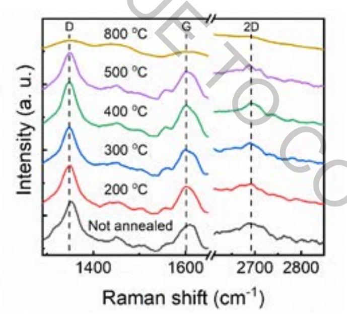
After annealing in Ar environment at temperatures, lower than 800°C, $I_{2D}/I_{G}$ ratio changed from 1.04 to 0.47 and $I_{D}/I_{G}$ ratio changed from 1.3 to 1.45, suggesting appearance of additional deformations. Annealing in $N_{2}$ environment, $I_{2D}/I_{G}$ changed from 1.6 to 0.62 and $I_{D}/I_{G}$ from 1.56 to 2.02 hinting a huge increase in defective sites and strain development. After investigating changes in Raman spectrum after annealing in vacuum we have found out that $I_{2D}/I_{G}$ changed from 0.61 to 0.23 and $I_{D}/I_{G}$ from 1.53 to 1.71, showing that the dominant effect is rather defect formation than reduction, however values indicate a large number of layers, which could lead to inconclusive estimations.