
GaN is a promising wide band-gap material for production of light-emitting diodes, high-electron-mobility transistors, high-frequency and high-power electronic devices, solar-blind photo-sensors and radiation tolerant particle detectors applied in high energy physics, radiation monitoring and other fields [1]. The wide band-gap of GaN determines a low leakage current. High luminescence efficiency is also an attractive characteristic of GaN in order to make the double response radiation sensors. In recent years, the formation of epitaxial GaN layers on Si substrates for various applications has gained a considerable interest due to the relatively low cost of Si substrates. In order to obtain high-quality GaN layers, the AlN buffer layer is deposited on Si beforehand. However, electrically active defects formed on the AlN/Si interface and Si surface may determine the functionality of the GaN based devices. In order to produce high-quality GaN-on Si devices, it is important to investigate the electrically active defects that are formed on the Si substrates.
The samples investigated in this work have been used as substrates for deposition of MOCVD AlN/AlGaN/GaN layers using different deposition pressure: 75 Torr (sample A) and 200 Torr (sample B). To measure recombination parameters of the interface and Si substrate, the top AlGaN/GaN layers were removed using inductively-coupled-plasma reactive ion etching (ICP-RIE) method. The recombination characteristics of the samples have been examined using a contactless technique of the microwave probed photoconductivity transients (MW-PC) by combining the bulk (${\lambda}_{ex}$=1062 nm) and surface (${\lambda}_{ex}$=531 nm) carrier injection regimes. The defects present in interfaces and Si substrates have been identified by deep level transient spectroscopy (DLTS) technique using junction structures formed on ICP-RIE etched samples.
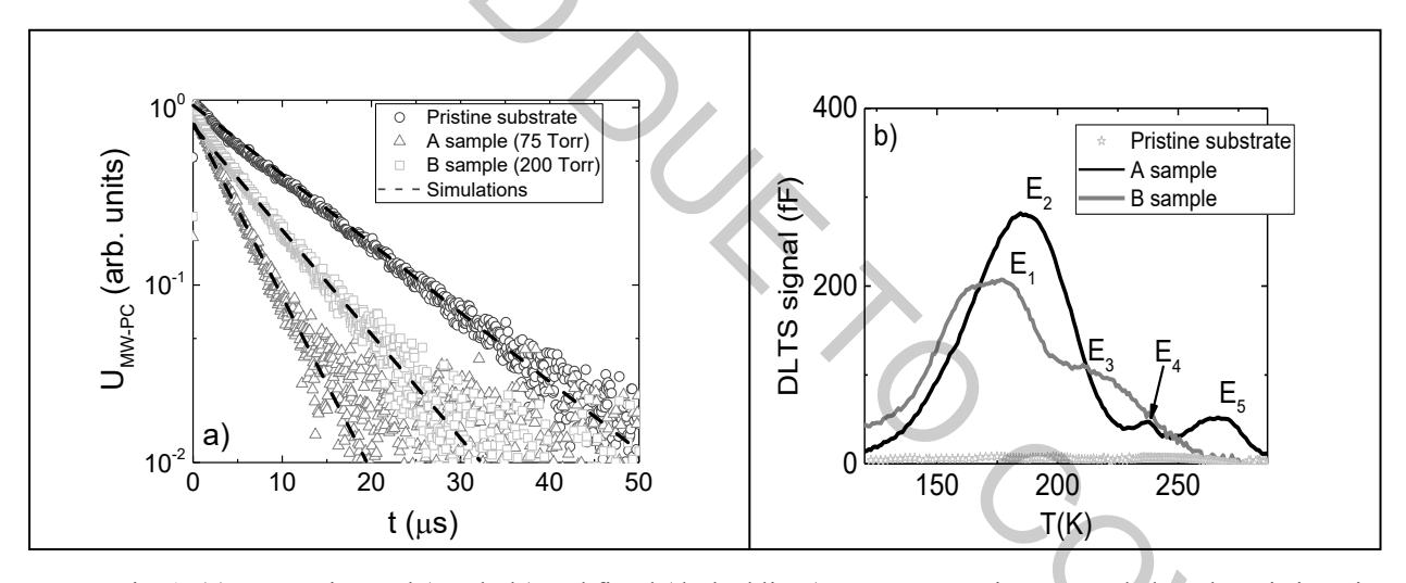
Analysis of the MW-PC transients allowed to determine the impact of deposition procedures of the AlN/AlGaN/GaN layers on the excess carrier lifetime. It has been found that the bulk carrier lifetime drops by the factor of 2.75 in A sample and by 1.75 in B sample relatively to the pristine Si substrates. The symmetry of the surface recombination velocities ($s_{0}$=$s_{d}$) has been revealed by measurements of $s_{0}$ and $s_{d}$ on both sides of the pristine substrate by exciting the opposite surfaces with strongly absorbed light pulses. The 3.5 times higher surface recombination velocity ($s_{0}$) has been determined on the AlN/Si interface side relatively to the Si substrate ($s_{d}$) for the GaN/AlGaN/AlN/Si structures. This indicates the enhanced defect concentration introduced by formation of the AlN/Si. The DLTS spectroscopy allowed us to identify the prevailing carrier traps and to extract their concentrations in AlN/Si interfaces and pristine Si substrates. It has been inferred that the concentration of the impurities and their complexes determined for the AlN/Si interfaces substantially prevails that obtained for the pristine Si substrates. The combined analysis of the MW-PC and DLTS characteristics as well as the extracted parameters of the carrier lifetimes and trap concentrations will be discussed.