
Copper selenide belongs to I–VI compound semiconductor materials. CuxSe (x = 1-2) thin films have been one of the most studied in recent years, with stoichiometric (Cu2Se, Cu3Se2, CuSe, and Cu2Se) and non-stoichiometric (Cu2-xSe) compositions exhibiting a continuous change of physical properties. CuxSe can been used in the fabrication of photovoltaic devices such as window materials, super ionic conductors, electro-optical devices, optical filters, thermo electric converters and photo electrochemical cells. Copper selenides can be formed on various substrates, such as glass, silicon, silicon oxide, titanium, various polymers, etc., using techniques, like chemical vapor deposition, chemical spray pyrolysis, atomic layer deposition or electrochemical deposition. All mentioned deposition methods usually require specialized equipment, vacuum, high temperature, use of electrolytes, it is hard to form layers across large surfaces, thus making them expensive and not suitable for all substrates.
Here is reported the preparation of electrically conductive CuxSe-PA films (PA – polyamide 6) by deposition of copper selenides from aqueous solutions on the PA film surface using Successive Ionic Layer Adsorption and Reaction (SILAR) method. This method used with the polymer differs from other methods, as it does not require specialized equipment or conditions, is cheap and simple, can be used at room temperatures. It has two stages: first – copper ions are adsorbed on polyamide surface from a precursor solution, containing copper ions, second – copper selenide layers are formed by treating the layer formed in the first stage with a solution containing selenium ions. The substrate is rinsed in distilled water after treatment in either solution.
Copper selenide thin films on the PA substrate were formed using the SILAR method at room temperature (20°C) and at 50°C. Their characterization was carried out through X-ray diffraction (XRD), scanning electron microscopy (SEM) and energy-dispersive X-ray spectroscopy (EDX).
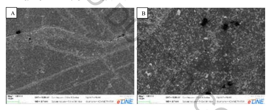
Observations about crystal size and homogeneity of CuxSe films can be made from the SEM images shown in Fig. 1. The size of the crystals deposited at 50°C is larger than the size of those deposited at 20°C. The film in image A appears to be more homogeneous than that of image B, due to a smaller variation of crystal sizes. From these observations, it can be concluded that at higher temperatures the rate of CuxSe crystal growth increases more than the rate of formation of crystal nucleation sites.
EDX results show an overall higher amount of copper selenide deposited at 50°C than 20°C, with copper to selenium ratio being 1.6 and 1.5 respectively. XRD analysis is not sensitive enough to show what phases of copper selenides formed on the sample treated at 20°C, however Cu2-xSe phase is observed on the 50°C sample.