GOLD PATTERNS ON n-SILICON SURFACE FOR SENSORIC APPLICATION
Victoria Bundyukova1, Dzmitry Yakimchuk1, Vladislav Prigodich1
1 Scientific-Practical Materials Research Centre of the NAS of Belarus, 220072 Minsk, Belarus
Silicon as a widely used semiconductor material, is used to a wide range of scientific and engineering applications, such as photovoltaic, nanoelectronic, sensitive biosensor devices, etc [1], [2]. The possibility of modifying silicon with various metals allows it to be used as the basis for sensor devices. Numerous works describe the method of electrodeposition of noble metals on the silicon surface to form a microrod array [3], [4]. However, this one has various limitations, including the size of the formed nanoparticles and morphology, the unevenness of the coating thickness, etc [5].
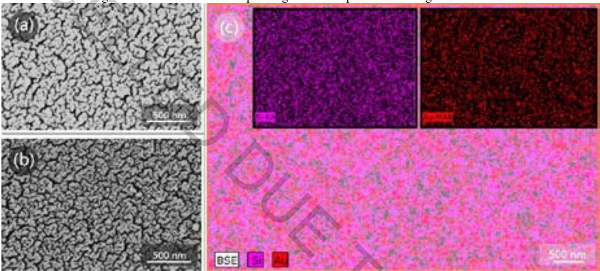
In this work, a galvanic deposition method was used to obtained gold nano patterns on a silicon surface of n-types from a salt of AuCl3 · (H2O) in aqueous solution at various temperatures. The concentration of gold ions in the initial solution was 0.01 M with the subsequent addition of 5 M HF acid in a 1:1 ratio. The morphological and structural properties of the resulting structures were studied depending on the temperature of the gold solution.
Fig. 1. SEM images of gold NSs on Si template deposited from AuCl3 solution at different temperatures: (a) – 25°C; (b) – 50 °C; (c) – EDX-map corresponding to the SEM image (a).
The obtained gold nanopatterns demonstrated the potential use for Raman signal amplification on a reference analyte Rhodamine 6G with a concentration of 10-6 M. Thus, there is a possibility of using gold nanotracks as SERS-active surfaces for sensors.
Acknowledgments: The authors acknowledge the support of the work in frames of H2020 - MSCA - RISE2017 - 778308 - SPINMULTIFILM Project, the Scientific-technical 'program Technology-SG' [project number 3.1.5.1].
[1] Wang, Y., Lu, N., Wang, W., Liu, L., Feng, L., Zeng, Z., ... Chi, L. (2013). Highly effective and reproducible surface-enhanced Raman scattering substrates based on Ag pyramidal arrays. Nano Research, 6(3), 159–166.
[2] Tripathy, A., Sen, P., Su, B., & Briscoe, W. H. (2017). Natural and bioinspired nanostructured bactericidal surfaces. Advances in Colloid and Interface Science, 248, 85–104.
[3] Fukami, K., Kobayashi, K., Matsumoto, T., Kawamura, Y. L., Sakka, T., & Ogata, Y. H. (2008). Electrodeposition of Noble Metals into Ordered Macropores in p-Type Silicon. Journal of The Electrochemical Society, 155(6), D443.
[4] Ogata, Y., Kobayashi, K., & Motoyama, M. (2006). Electrochemical metal deposition on silicon. Current Opinion in Solid State and Materials Science, 10(3-4), 163-172.
[5] Tonelli, D., Scavetta, E., & Gualandi, I. (2019). Electrochemical Deposition of Nanomaterials for Electrochemical Sensing. Sensors, 19(5), 1186.