
Silicon carbide is an attractive semiconductor for high power, high temperature, and high frequency electronic devices due to its superior properties [1]. An important task is the integration of SiC devices and silicon circuits within the traditional VLSI technology [1, 2]. Productive and inexpensive methods of growing the material should be developed to achieve the task. The growth of SiC/Si structures faces the problems of large lattice mismatch and very different thermal expansion constants which result in formation of dislocations, twins and stacking faults. Raman scattering is a powerful and nondestructive tool, which can be used for identifying the polytype structure of SiC as well as for stress and defect analysis. In this work, we applied Raman scattering to investigate epitaxial thin SiC layers grown during rapid thermal carbonization (RTC) of the Si wafer under high vacuum conditions.
SiC layers were grown on Si (100) by reacting Si wafer with residual carbon atmosphere at 1100 °C for 30 sec. The pressure in the chamber was about 1·10-2 Pa. Si (100) wafers were pre-cleaned in the 5% HF: H2O solution, and rinsed in deionized water. The structural properties of SiC/Si were investigated by Raman spectroscopy in backscattering configuration at room temperature with a Raman confocal microscope Nanofinder High End (Lotis TII, Belarus-Japan). Solid-state lasers at 473 or 532 nm were used for excitation. To clearly resolve the signal from SiC layer, a window in the Si substrate was etched away in HF/HNO3 solution.
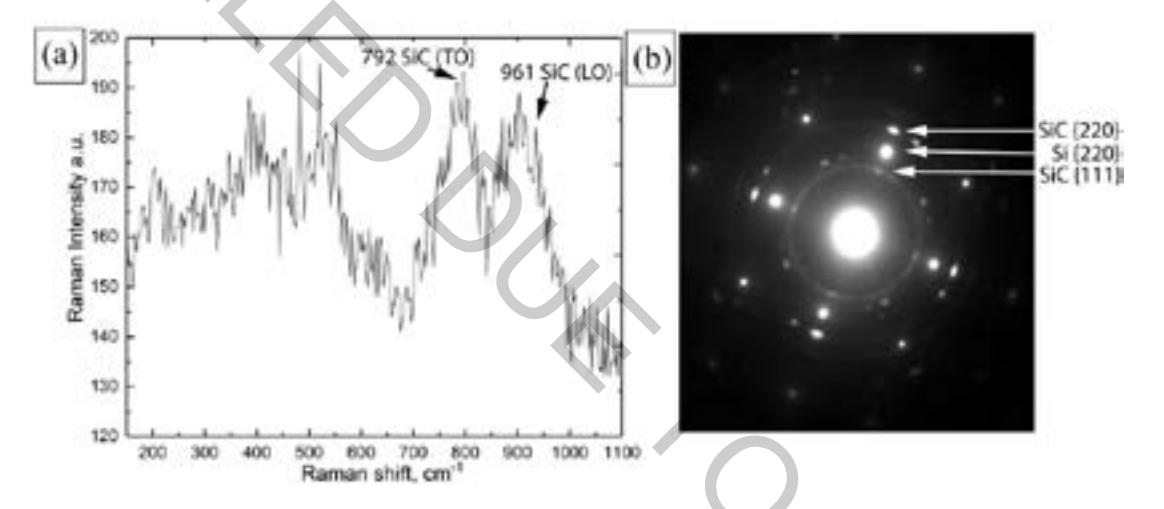
A typical Raman spectrum of the SiC layer RTC grown at 1100 °C is presented at figure 1a. The spectrum shows two peaks in the 750-800 cm-1 and 961 cm-1 range which indicate the 3C polytype of SiC. The peaks at 792 cm-1 and 961 cm-1 (arrows) correspond to transverse (TO) and longitudinal (LO) optical phonon modes, respectively. The broadening of the TO band (792) is, probably, indicative of stacking faults [3] or other defects such as anti-phase boundaries and dislocations [4]. The high structural quality of the SiC layer is confirmed by the transmission electron diffraction (Fig. 1b). In the diffraction pattern, the intensity of the polycrystalline diffraction rings is extremely low. Diffraction spots (SiC(220) and SiC(111)) correspond to the 3C SiC polytype. It could be concluded that thermal treatment of Si wafer at 1100 °C in a residual carbon atmosphere results in epitaxial growth of high quality thin silicon carbide layers.