
Hybrid perovskites are attractive due to their high carrier mobility [1], diffusion length [2], large crystal grains, tunable bandgap and inexpensive production via spin-coating. Impressive results have been demonstrated in conditions similar to those in optically-pumped lasers [3], [4]. In spite of this, the perovskite phase can degrade rapidly due to humidity and high excitation density induced ion migration. To increase stability for applications the 2D perovskite (2DP) phase has been developed. Organic ligand layers in 2DP separate crystalline perovskite nanosheets of average thickness n (in units of lattice period), thus inducing quantum confinement for the generated carriers. This leads to higher bimolecular recombination, however, a reduction in perovskite absorption is present, raising the amplified spontaneous emission (ASE) threshold ${\Delta}n_{ASE}$. In this work, we optimised the 2DP layer dimensionality n for characteristics appropriate to a laser medium in PEA2FAn-1PbnBr3n+1 perovskites.
Sample preparation was done in collaboration with Kyushu University. Prior to use, ultrasonication followed by ultraviolet-ozone treatment were used to clean quartz substrates. The precursor solutions consisted of dissolved phenetylammonium bromide (PEABr), formamidinium bromide (FABr) and lead bromide (PbBr) in various ratios. Thus, 2DP dimensionalities of n = 1, 2, 3, 4 and $\infty$ (3D) were achieved. The spin-coated layers were encapsulated between 2 quartz substrates using epoxy glue.
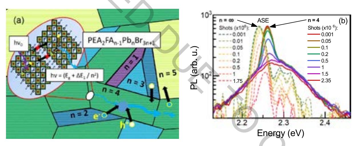
As seen in Fig. 1 (a), the 2DP bandgap gets a larger blueshift in lower dimensionalitites n, that is ${\Delta}E_{\varrho} \propto 1/n^2$. Also, perovskite domains composed of crystallites with various thicknesses ncryst form in the layers [5], not necessarily $n = n_{cryst}$. This, together with random domain orientations prevents population inversion within a single desired band to appear in the 2DP layers, as excited carriers tend to funnel through crystallite surface boundaries into states of lower energy. Thus, ASE lines with thresholds ${\Delta}n_{ASE} = 1.72$ and 1.53 (x1018cm-3) appear in n = 4 and $\infty$ respectively, i.e. in samples of smaller quantum confinement, more beneficial for a homogenous phase to form. Even though at low excitation intensity samples n = 1, 3 have higher external quantum yields (EQE = 1.1%, 1.7%), at higher excitations (for example, ${\Delta}n = 2{\Delta}n_{ASE}$) n = 4 catches up with an EQE $\approx 20\%$. In addition, the 2DP phase endures longer in an active ASE regime compared to the 3D perovskite (Fig. 1 (b)). So, the 2D perovskite with dimensionality n = 4 seems best fit for the role of a laser active medium, given future domain orientation unification during the production process.