
Recently, the infrared (IR) spectral region has attracted huge attention. Due to a number of vibrational absorption lines of organic molecules, IR becomes very important for applications in various areas, such as biomedicine, life and environmental sciences. For example, Light identification and ranging (LiDAR) called Frequency-Modulated Continuous-Wave LiDAR require narrow linewidth laser of the sub-MHz range and high power (up to 200 mW at 1550 nm). New emerging field of quantum cryptography requires single-frequency lasers at 785 nm for sending encoded information over the fiber networks and from nano-satellites down to Earth. High power, high brightness and narrow-line 785 nm lasers are on demand in Raman Spectroscopy for industrial setups and remote environmental contamination measurements. However, most of these applications are limited by the lack of efficient semiconductor IR sources and detectors. High temperature operation of semiconducting lasers is limited by losses due to non-radiative Auger recombination. Thus, the engineering and study of new materials functioning at room temperature in IR is still important and challenging. The research focuses on two objectives: first, low power, small size and weight NIR sources for applications in wireless sensing systems and, secondly, narrow linewidth and high power NIR lasers for remote applications. In this work, A3B5 compounds were used into the active area of NIR emitters operating up to 860 nm, while bismide-based A3B5 MQW structures, exhibiting strong energy bandgap reduction (70 to 90 meV/%Bi) and increased spin-orbit splitting energy ASO [1, 2] as well as lower temperature sensitivity [3, 4], have been employed in sources covering the 1.0 μm -1.55 μm wavelength region.
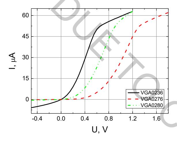
The diode structures were grown by molecular beam epitaxy (MBE) under optimized growth condition onto n-GaAs(100) substrate. Both the n-type and p-type AlGaAs waveguide layers were of 1.5 μm thickness and doped of 1×1018 cm-3 by silicon and beryllium, respectively. The surface morphology of the structures examined by atomic force microscopy (AFM), optical properties evaluation by measuring room-temperature photoluminescence. Grown structures were processed using UV photolithography. As-cleaved electrical properties of LDs and LEDs were investigated using Keithley 4200 semiconductor characterization system and Cascade Microtech Summit probe station. DC, pulsed current-voltage (I-V, pulsed I-V, see Fig. 1) and capacitance-voltage (C-V) dependences were measured in air at room temperature. Closed chamber was used to avoid illumination of the samples.