
Graphene is notorious two-dimensional material, consisting of one or a few layers of sp2 bonded carbon atoms distributed in honeycomb crystal lattice. Unique properties of graphene such as high electron and hole mobility, thermal conductivity, mechanical resistance, tunable bandgap and more makes it focus of both fundamental and applied scientific research [1], [2]. While mechanically exfoliated graphene exhibits best performance when incorporated in devices, this type of graphene is hardly obtainable in large areas and mass quantities [3]. Moreover, device fabrication requires transfer step during which graphene is contaminated by adsorbents, wrinkles and potentially cracks [4].
In present work, few layer graphene is produced by annealing amorphous carbon – nickel (a-C:Ni) and amorphous carbon – cobalt (a-C:Co) thin film composites, deposited by magnetron co-sputtering. Relative carbon and transition metal concentrations and film thicknesses were varied to find optimal sputtering conditions for graphene formation. Raman spectroscopy as well as X-ray diffractometry and X-ray photoelectron spectroscopy were used to characterize graphene and film phase. Residual metal was treated with appropriate etchants (ceric ammonium nitrate for nickel composites and chloric acid for cobalt composites). From fig. 1 it is evident that few-layer graphene formed on both post-annealed a-C:Ni and a-C:Co films. However, cobalt composites exhibit less defects (lower D band) and smaller number of layers (higher $I_{\rm 2D}/I_{\rm G}$ ratio).
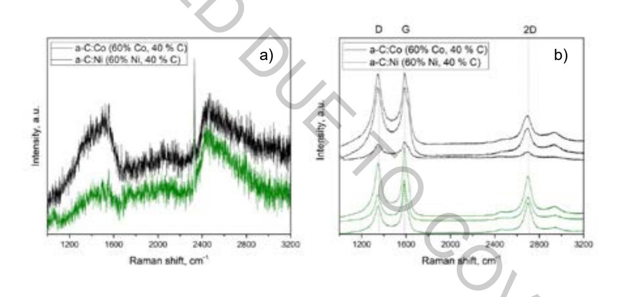
These results are promising as graphene formed through a-C:Co composite carbon segregation process can be used for graphene-silicon Schottky diode production.